Metasurfaces are revolutionizing the field of optics innovation, offering unprecedented capabilities in light manipulation and device design. Developed through cutting-edge research, these ultra-thin surfaces can focus light all while being smaller and cheaper than traditional lenses, making them ideal for applications in consumer electronics. The startup Metalenz, co-founded by Rob Devlin and born from Harvard’s Capasso lab, has emerged as a leading manufacturer of these groundbreaking mini-lenses. With millions of metasurfaces now integrated into popular devices like the iPad and Samsung Galaxy S23 Ultra, the potential of this technology is being realized on a massive scale. The versatility of polarization metasurfaces further emphasizes their significant role in advancing visual and sensing technology, transforming how we interact with our devices in everyday life.
Alternative optical elements, often referred to as synthetic lenses or engineered light-manipulating surfaces, are garnering attention for their disruptive potential in the lens manufacturing domain. These innovative optics, developed at the intersection of research and industry, are at the forefront of redefining how light is utilized across various devices. Through advancements like mini-lenses, companies are maximizing efficiency and minimizing size, thereby enhancing the functionality of modern smartphones and cameras. The emergence of firms like Metalenz highlights a new era in optics technology, where traditional glass lenses are being supplanted by these sophisticated metasurfaces. As the adoption of these transformative devices continues to grow, the implications for consumer electronics and beyond are profoundly exciting.
The Evolution of Mini-Lens Technology
Mini-lens technology has undergone a remarkable evolution since its inception, largely propelled by cutting-edge research in optics innovation. Spearheaded by Rob Devlin and his team at Metalenz, these mini-lenses have revolutionized how light is manipulated in consumer electronics. Initially conceived during Devlin’s doctoral studies at Harvard, the concept of using arrays of tiny pillars on a thin wafer to focus light marks a departure from traditional lens designs. Metalenz’s production of millions of these new devices underscores their commitment to efficiency and mass production in a market that demands higher innovation with less physical bulk.
As manufacturers seek ways to incorporate more advanced features into smartphones and tablets, the shift from conventional lenses to mini-lenses provides a significant advantage. Unlike bulky glass components, mini-lens technology offers a much smaller footprint without sacrificing optical quality, making it ideal for modern consumer electronics. The widespread implementation of these devices has enabled products not only to be sleeker but also to contain advanced functions such as depth sensing and augmented reality capabilities. This advancement continues to disrupt the conventional lens industry and redefine product design standards across technology sectors.
Discovering Polarization Metasurfaces
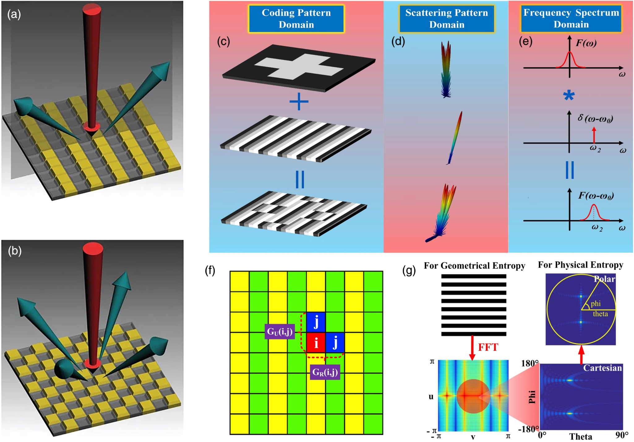
Polarization metasurfaces represent an exciting frontier in optics innovation, offering sophisticated capabilities that traditional lenses cannot provide. These advanced surfaces utilize the unique properties of light polarization to create new functionalities for devices, particularly in consumer electronics. For instance, Metalenz’s pioneering work in developing polarization metasurfaces promises to enhance the security of smartphone applications, providing a lower-cost alternative to existing options that utilize large, costly polarization cameras. This technology’s compact nature allows it to fit seamlessly into a variety of devices, from smartphones to wearable technologies.
The significance of polarization in tech applications extends beyond just security; it encompasses a wide array of potential uses that exploit how different materials interact with polarized light. By harnessing specific polarization signatures, devices can achieve more accurate measurements and detections, which has substantial implications for fields such as health monitoring and environmental sensing. With their focus on innovating within this realm, Metalenz is at the forefront of integrating these capabilities into everyday consumer products, thus illustrating the transformative power of metasurfaces in shaping future technologies.
Rob Devlin’s Vision and Leadership
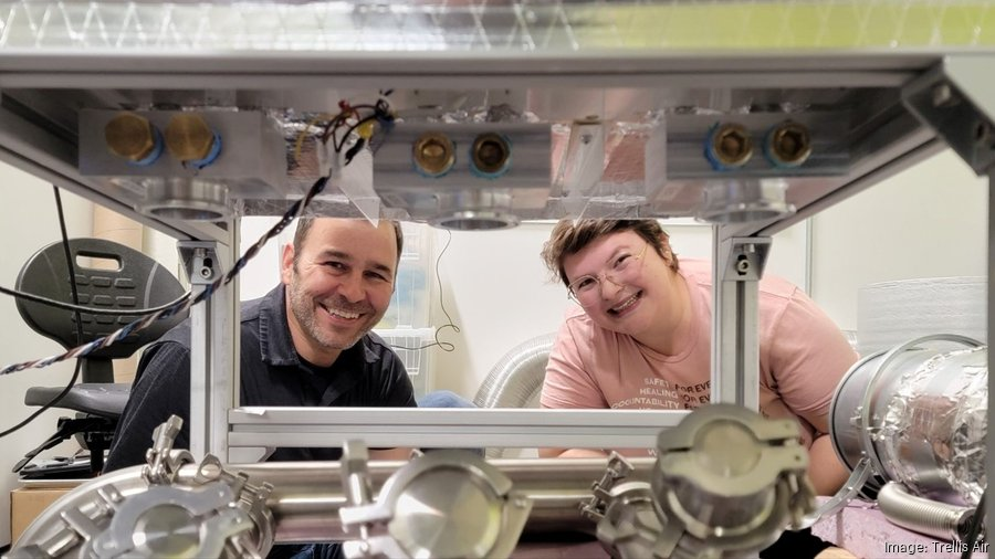
Rob Devlin’s vision for Metalenz is deeply rooted in a commitment to optics innovation and the potential for disruption in the consumer electronics market. His leadership has been pivotal in transitioning research prototypes from academic laboratories into commercially viable products. Under his guidance, Metalenz has not only achieved mass production of mini-lenses but has also set ambitious goals for developing groundbreaking technologies such as Polar ID. Devlin’s understanding of materials science and nanofabrication continues to drive the company’s progress, positioning it as a leader in the industry.
Moreover, Devlin’s collaboration with Federico Capasso, a co-founder and professor at Harvard, bridges academia and industry, allowing for an innovative exchange of ideas and continual refinement of their products. Under Devlin’s leadership, the company has also focused on enhancing existing technologies while exploring new applications for metasurfaces, ensuring that they maintain a competitive edge in a rapidly evolving tech landscape. His strategic approach reflects a broader commitment to harnessing the potential of university research to create impactful industries, a vision articulated by former Harvard President Drew Faust.
Impact of Metasurfaces on Consumer Electronics
Metasurfaces are drastically changing the landscape of consumer electronics, offering innovative solutions that drive product efficiency and functionality. With companies like Metalenz pushing the boundaries of optics through the deployment of metasurfaces, users can benefit from advanced technologies such as 3D sensing and augmented reality features in slim, lightweight devices. This transformation is vital as consumer electronics continue to evolve, demanding more sophisticated functionalities while simultaneously minimizing space requirements. The successful integration of these metasurfaces into popular devices, including the latest iPad and flagship smartphones, demonstrates their widespread acceptance and utility.
Furthermore, the impact of metasurfaces extends beyond mere aesthetic improvements; it enhances overall device performance by providing better imaging capabilities and facilitating advanced security applications. As the demand for nuanced sensor technology increases, the ability to integrate functionalities without adding significant bulk becomes crucial. The adoption of metasurfaces allows manufacturers to meet these challenges effectively, ensuring they stay competitive in a fast-paced market driven by continuous advancement and innovation.
The Future of Light-Focusing Technologies
The future of light-focusing technologies is undoubtedly bright, propelled by the ongoing advancements in metasurface applications. With their potential to miniaturize traditional optical components, these technologies promise to revolutionize industries ranging from consumer electronics to healthcare. The continuous refinement and development of light-focusing metasurfaces are set to inspire innovations that were previously limited by the physical constraints of traditional lenses. As Metalenz and similar companies expand their reach, the implications of these technologies will reshape how we perceive and interact with the digital world.
As researchers like Rob Devlin lead the charge in enhancing these technologies, we may soon see widespread adoption of optics innovations that incorporate new functionalities, including precision sensing and advanced imaging techniques. Industries are likely to experience rapid transformations as companies leverage the capabilities offered by compact and efficient metasurfaces. This impending technological evolution not only promises to enhance user experiences but also opens up new avenues for product development in diverse fields, from virtual reality to smart health monitoring systems.
Challenges in Scaling Metasurface Production
Despite the exciting potential of metasurfaces in consumer electronics, scaling their production poses unique challenges. The manufacturing process for these advanced optics requires sophisticated technology and precise techniques that can ensure quality and consistency across millions of units. Companies like Metalenz must navigate these challenges while striving to meet increasing demand, which necessitates collaboration with established semiconductor foundries to leverage their large-scale production capabilities. The transition from laboratory prototypes to mass production requires rigorous testing and validation to guarantee that the final products meet industry standards.
Moreover, maintaining the delicate balance between innovation and cost-efficiency is paramount in the competitive tech market. As more businesses recognize the value of metasurfaces, pricing strategies will need to adapt in order to remain attractive to consumers. This necessitates continuous investment in research and development, where advancements not only focus on optimizing manufacturing processes but also enhancing product functionalities. The ability to effectively scale production without compromising on quality will be critical for the success of metasurfaces in commercially viable applications.
Applications of Mini-Lenses in Modern Devices
The applications of mini-lenses in modern devices are vast and varied, reflecting their versatility and functionality in today’s tech landscape. From enhancing the capabilities of smartphone cameras to improving depth-sensing technologies in augmented reality applications, mini-lenses are becoming integral components in many devices. Their design, characterized by the use of metasurfaces, allows manufacturers to create products that are not only slim and lightweight but also packed with advanced features that traditional optics often struggle to provide. This newfound capability enhances user experiences by integrating richer functionalities without adding cumbersome weight or size.
In addition to augmenting imaging capabilities, mini-lenses are being employed in a variety of other fields, including automotive safety and robotics. For example, utilizing mini-lenses in proximity sensors and facial recognition systems can improve the accuracy and efficiency of these technologies. As consumer electronics continue to embrace mini-lens technology, we can expect to see innovative applications that leverage their unique properties to solve complex challenges across different industries. By continually exploring new uses for these devices, companies like Metalenz are defining the future of optics in consumer products.
The Role of Collaboration in Optics Innovation
Collaboration plays a pivotal role in the ongoing advancement of optics innovation, particularly in the development of metasurfaces and mini-lens technology. The partnership between academia and industry exemplified by the founding of Metalenz is a prime instance of how cross-disciplinary efforts can lead to groundbreaking products. The synergy between researchers in federated labs and engineers in startups fosters an environment ripe for innovation, as it combines theoretical knowledge and practical application. These collaborations not only drive technological advancements but also enrich the talent pool within companies as they integrate diverse skill sets into their teams.
Furthermore, collaboration extends beyond initial product development; it encompasses ongoing relationships that sustain continued innovation. By maintaining ties with academic institutions, companies like Metalenz can quickly adapt to new research findings and implement cutting-edge techniques into their production processes. This adaptive approach helps ensure that they remain competitive in a rapidly changing market, where the ability to pivot and incorporate the latest innovations into product lines can mean the difference between success and stagnation.
Sustainability and Future Developments in Metasurface Technology
As the technology behind metasurfaces progresses, sustainability emerges as an increasingly vital consideration within the field of optics innovation. The push towards environmentally friendly manufacturing processes and materials is crucial, especially in consumer electronics, where production can contribute significantly to ecological footprints. Metalenz, along with other industry players, is committed to finding ways to reduce waste and energy consumption during production, ensuring that the scaling of metasurface technology aligns with sustainable practices. Furthermore, minimizing the physical space required for components, thanks to mini-lens technology, inherently promotes a more sustainable design philosophy.
Future developments are poised to further emphasize sustainability as a core value in the production of metasurfaces. Research into biodegradable materials or those that require less energy to process could revolutionize how these optics are manufactured. As societal pressure mounts for companies to adopt eco-friendly practices, the investment in sustainable technologies will not only benefit the environment but also resonate with consumers who increasingly prioritize such values when making purchasing decisions. The pathway towards sustainable metasurface technology signifies a broader commitment to responsible innovation within the optics industry.
Frequently Asked Questions
What are metasurfaces and how do they relate to mini-lens technology?
Metasurfaces are engineered surfaces composed of nanostructures that manipulate light in novel ways. Related to mini-lens technology, they allow for the creation of ultra-thin lenses that can focus light similar to conventional lenses, but with greater efficiency and compactness. This innovation, pioneered by researchers like Rob Devlin in the Capasso lab, revolutionizes traditional optics by embedding these devices in consumer electronics.
How do polarization metasurfaces enhance security in consumer electronics?
Polarization metasurfaces leverage the unique polarization properties of light to add an additional layer of security for devices like smartphones. By analyzing the polarization signature of objects, these metasurfaces can help distinguish between genuine users and replicas, reducing the risk of spoofing attacks. This innovation is set to make security features more accessible and cost-effective than traditional systems.
What are the advantages of using metasurfaces over conventional lenses in optics innovation?
Metasurfaces offer several advantages over conventional lenses, including a significant reduction in size and weight, lower manufacturing costs, and enhanced performance. These ultrathin light-focusing devices can be produced using existing semiconductor fabrication techniques, which allows for mass production in consumer electronics and supports advanced features without the bulk of traditional optical components.
How has Metalenz contributed to the field of consumer electronics with metasurface technology?
Metalenz, founded by Rob Devlin, has made significant strides in the field of consumer electronics by mass-producing light-focusing metasurfaces. Their devices are now embedded in popular products like the iPad and smartphones, improving imaging capabilities and enabling advanced features such as 3D sensing and facial recognition with superior efficiency over traditional optical systems.
What implications does the development of Polar ID using polarization metasurfaces have for future technology?
The development of Polar ID using polarization metasurfaces has vast implications for future technology, including enhanced security in mobile devices, improved biometric recognition capabilities, and new medical diagnostic applications. By significantly reducing size and costs, these innovations can be integrated into a wider range of consumer products, transforming how we interact with technology and enhance safety.
What role did Rob Devlin play in the innovation of metasurfaces at Harvard’s Capasso lab?
Rob Devlin was instrumental in the innovation of metasurfaces during his doctoral studies at Harvard’s Capasso lab. He developed new mini-lens prototypes and worked on refining the design and fabrication processes, ultimately leading to the establishment of Metalenz, which commercializes these groundbreaking devices in various consumer electronics.
| Key Aspect | Details |
|---|---|
| Rob Devlin’s Role | Developed mini-lens during PhD, now CEO of Metalenz producing millions of optical metasurfaces. |
| Metasurfaces Description | Small, cheap devices that bend light using tiny pillars on a wafer; mass-produced in semiconductor foundries. |
| Commercial Success | 90 million metasurfaces installed in consumer electronics like iPad, Galaxy S23 Ultra, and Pixel 8 Pro. |
| Innovation Origin | Based on research by Federico Capasso’s lab since 2007; transitioned from prototypes to production rapidly. |
| Impact on Industry | Disrupts conventional lens manufacturing; allows for sleek designs in modern devices. |
| Future Developments | Polar ID technology utilizing light polarization for enhanced security in smartphones and more. |
| Growth and Workforce | Company doubled workforce to 45; focused on enhancing existing products and exploring new applications. |
Summary
Metasurfaces are at the forefront of optical technology, representing a groundbreaking evolution in lens design and manufacturing. Originating from advanced research at Harvard, these tiny yet powerful devices harness nanostructures to bend light with unprecedented efficiency, enabling new functionalities in consumer electronics. As the industry shifts towards sleeker and more compact devices, metasurfaces offer a compelling alternative to traditional optics, paving the way for innovative applications in security, imaging, and beyond. The ongoing developments in metasurface technology, including features like Polar ID for enhanced security, exemplify the potential for transformative impacts across multiple sectors.